Datasheet4U.com - NCV51510

NCV51510 Datasheet, ON Semiconductor

NCV51510 Datasheet, ON Semiconductor

Page 1 of NCV51510 Page 2 of NCV51510 Page 3 of NCV51510

NCV51510 regulator equivalent

  • termination source / sink regulator.
  • Preview is limited to up to three pages.

NCV51510 Features and benefits

NCV51510 Features and benefits


* Generate DDR Memory Termination Voltage (VTT)
* For DDR, DDR−2, DDR−3 and DDR−4 Source / Sink Currents
* Supports Loads Up to ±3 A (Typ), Output is Over−Cur.

NCV51510 Application

NCV51510 Application

Requiring Unique Site and Control Change Requirements; AEC−Q100 Qualified and PPAP Capable*
* This is a Pb−Free Devi.
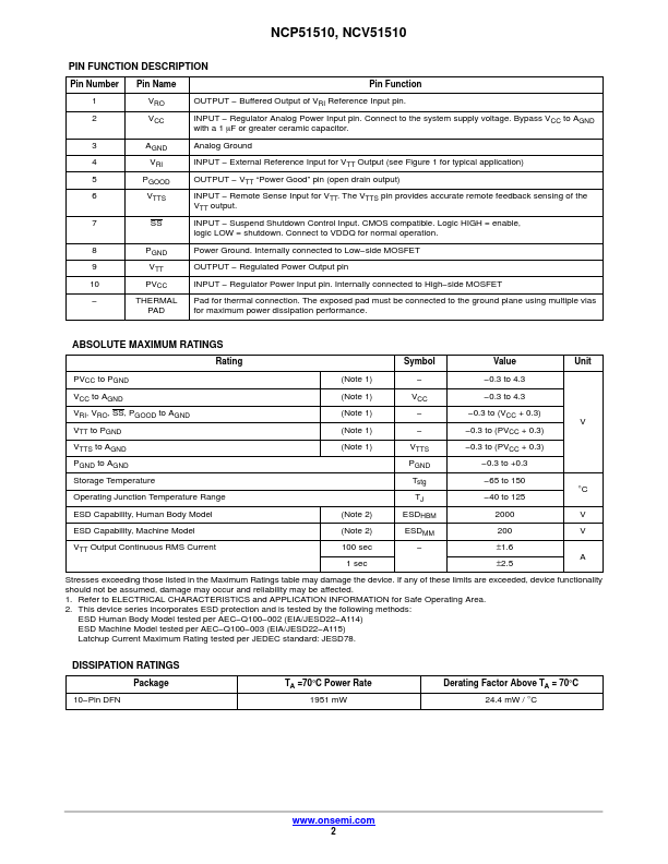
NCV51510 Description

NCV51510 Description

Pin Number Pin Name Pin Function 1 VRO OUTPUT − Buffered Output of VRI Reference Input pin. 2 VCC INPUT − Regulator Analog Power Input pin. Connect to the system supply voltage. Bypass VCC to AGND with a 1 mF or greater ceramic capacitor. 3 AGND.

Image gallery

Page 1 of NCV51510 Page 2 of NCV51510 Page 3 of NCV51510

TAGS

NCV51510
Termination
Source
Sink
Regulator
ON Semiconductor

Manufacturer


ON Semiconductor (https://www.onsemi.com/)

Related datasheet

NCV51511

NCV51513

NCV51561

NCV5104

NCV5106A

NCV5106B

NCV511

NCV51152

NCV51190

NCV51198

Since 2006. D4U Semicon.   |   Datasheet4U.com   |   Contact Us   |   Privacy Policy   |   Purchase of parts